MOS integrated circuit
Type
According to the channel conductivity type of the transistor, it can be divided into P-channel MOSIC, N-channel MOSIC, and complementary MOSIC that combines P-channel and N-channel MOS transistors into one circuit unit. They are called PMOS, NMOS and CMOS integrated circuits. With the development of process technology, CMOS integrated circuits have become the mainstream of integrated circuits, and the process has become increasingly sophisticated and complex, from P-well or N-well CMOS to double-well CMOS technology. In the 1980s, a BiCMOS integrated circuit structure that combines the advantages of bipolar circuits and complementary metal-oxide-semiconductor (CMOS) circuits appeared. According to the gate material, it can be divided into lead gate, silicon gate, silicide gate and refractory metal (such as molybdenum, tungsten) gate and other MOSIC. The gate size has changed from micron to sub-micron (0.5-1 micron) and strong sub-micron ( 0.5 microns or less). In addition, MOSIC with different MOS integrated circuit structures has been developed: such as floating gate avalanche implanted MOS (FAMOS) structure for rewritable read-only memory; diffuse self-aligned MOS (DMOS) structure and V-groove MOS The structure, etc., can meet the requirements of high speed and high voltage. In recent years, a CMOS structure with sapphire as the insulating substrate has been developed, which has the advantages of anti-radiation, low power consumption and high speed. MOSIC is widely used in the fields of computer, communication, electromechanical instrument, home appliance automation, aerospace, etc. It can make the whole machine smaller in size, fast working speed, complex function, high reliability, low power consumption and low cost.
Advantages
①Simple manufacturing structure and convenient isolation.
②Small circuit size, low power consumption, suitable for high-density integration.
③The MOS tube is a bidirectional device with high design flexibility.
④Has the unique ability of dynamic work.
⑤Good temperature characteristics. Its disadvantages are low speed and weak driving capability. It is generally believed that MOS integrated circuits have low power consumption and high integration, and are suitable for digital integrated circuits; bipolar integrated circuits are suitable for high-speed digital and analog circuits.
R&D and promotion
In the late 1960s and early 1970s, my country’s research on integrated circuit technology has just started, only the development of bipolar small-scale integrated circuits has begun and a small amount of Production. At that time, foreign MOS circuits developed rapidly. Compared with bipolar circuits, MOS integrated circuits had the advantages of simple circuit, low power consumption, and high integration. However, there were still many difficulties in the research and development of domestic MOS integrated circuit technology. One difficulty is that MOS devices are easily broken down by static electricity. Some people describe it as: "MOS, MOS, it will die when touched"; another difficulty is that the gate oxide charge of MOS devices is not easy to control, which greatly affects the productivity of MOS circuits. And work stability. Therefore, everyone still has many doubts about the development prospects of MOS integrated circuits.
Under this situation, Comrade Xu Jiasheng from the semiconductor workshop led more than a dozen middle-aged and young teachers. Since 1970, he has resolutely devoted himself to the research, development and application promotion of MOS integrated circuits in my country. In the absence of technical materials and process equipment, and the production conditions were very backward, everyone was self-reliant and united to solve the problems of gate oxide charge and electrostatic damage protection from the process and circuit design, which helped the development of MOS integrated circuits in my country. Cleared the technical barriers. On this basis, we successfully developed small and medium-sized MOS numerical control circuits, including counters, registers, decoders, various flip-flops, gate circuits, etc., and produced them in small quantities. In order to promote these circuits, they also produced frequency counters, digital displays and other application components, and demonstrated them to relevant units to help solve technical problems in the application. In this way, MOS integrated circuits are finally recognized by the society. During this period, the Beijing Semiconductor Device No. 5 Factory, Qianmen Device Factory, Shanghai Device No. 5 Factory, Tianjin No. 1 Semiconductor Factory, Shijiazhuang Semiconductor Device Factory, Baoding Radio No. 2 Factory, etc. successively produced this series of circuits. These CNC series circuits have become the main products of many semiconductor factories for a long time. In addition to sending people to teach and promote technology, Tsinghua Semiconductor Workshop has also held several short training courses to help these companies train their production technology backbones. It can be said that Tsinghua's semiconductor workshop has become the earliest birthplace of MOS integration technology in my country.
Based on the successful development and promotion of small and medium-sized MOS numerical control series circuits, the semiconductor workshop has further advanced to medium and large-scale MOS integrated circuits, and has successfully developed a complete circuit of 050 desktop computers (devices), 2240 bits 96 A variety of large-scale integrated circuits such as character generators and 1KDRAM. From 1970 until 1976, Tsinghua has maintained the highest level of MOS integrated circuit technology in China.
Production conditions
In addition to the integrated circuit technology itself, the semiconductor workshop has also played an important role in promoting the development of my country's basic conditions for integrated circuit production. In order to meet the high-precision and automation requirements of large-scale integrated circuit production, many key equipment are self-made, such as high-precision shrinking machine, diffusion furnace and trichloroethylene oxidation system, high-speed homogenizing machine, plasma etching machine Etc. Some equipment is produced by the semiconductor workshop with performance requirements and trial improvements, and is produced in collaboration with other units. For example, the high-precision step-by-step repetitive compacting machine is produced in collaboration with the Radio Department and the Precision Instrument Department of our school. It is the equipment commonly used by domestic integrated circuit factories at that time.
In order to meet the requirements of large-scale integrated circuit manufacturing to reduce dust and contamination, the semiconductor workshop designed, purchased materials, and contacted the construction by itself. The original 800 square meter laboratory was purified and transformed in 1975. An ultra-clean workshop with 350 square meters and a purification level of 1000 and 10000 has been built. This was the first ultra-clean workshop used in the production of integrated circuits in China at that time. It met the needs of large-scale integrated circuit development and was used until 1993.
Use operating guidelines
1 Do not exceed the limits of the extreme working conditions listed in the manual.
2 All free input terminals on the device must be connected to VDD or VSS, and they must be in good contact.
3 All low-impedance devices (such as pulse signal generators, etc.) must be connected to the power supply before they are connected to the input of CMOS or NMOS integrated circuits. The device can only be disconnected after the same device is disconnected from the device. Power supply.
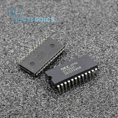
4 The printed circuit board containing CMOS and NMOS integrated circuits is only an extension of the device, and also requires compliance with operating guidelines. Connecting directly from the connector on the edge of the printed circuit board to the device can also cause damage to the device. General plastic packaging must be avoided. The address input or output of the CMOS or NMOS integrated circuit on the printed circuit board connector should be connected in series with a resistor. The delay time is increased due to the time constant of these series resistance and input capacitance. This resistance will limit the static high voltage damage caused by the movement of the printed circuit board or the contact with static-prone materials.
5 All CMOS and NMOS integrated circuits must be stored and transported in containers made of antistatic materials. Devices cannot be inserted into plastics or placed in ordinary plastic trays until they are ready for use. Can be taken out of the antistatic material container.
6 All CMOS and NMOS integrated circuits should be placed on a well-grounded workbench. Since the staff can also discharge static electricity on the workbench, the staff must be grounded before operating the device. It is recommended that the staff use a strong conductive belt to connect the wrist or elbow to the surface of the workbench well.
7 Nylon or other materials prone to static electricity are not allowed to come in contact with CMOS and NMOS integrated circuits.
8 In the process of automated operation, due to the movement of the device, the movement of the conveyor belt and the movement of the printed circuit board may generate high static voltage, so ionized air blowers and humidifiers should be used in the workshop Keep the indoor relative humidity above 35%. All the top, bottom, and side parts of the equipment that can be in contact with the integrated circuit should be made of grounded metal or other conductive materials.
9 The freezer compartment should be cooled with carbon dioxide, and a partition should be placed, and the device must be placed in a container of conductive material.
10 When it is necessary to straighten the outer leads and use manual soldering, the wrist should be grounded, and the solder tank should also be grounded.
11 The following measures should be taken during wave soldering:
a. The solder tank and conveyor belt system of the wave soldering machine must be grounded.
b. The workbench is covered with a conductive top cover and must be grounded.
c. The staff must follow the precautionary guidelines.
d. The finished workpiece should be placed in an anti-static container and sent to the next process first.
12 The following measures should be used to clean the printed circuit board:
a, the vapor degreasing agent and the basket must be grounded, and the staff must also be grounded.
b. Brushes and sprayers are not allowed to clean printed circuit boards.
c. The workpieces taken out of the cleaning basket should be immediately put into the steam degreaser.
d. High-speed air and solvents are allowed to be used only after the workpiece is well grounded or a static eliminator is used on the workpiece.
13 Must have the permission of the production line supervisor to use the static monitor.
14 It is not allowed to insert or remove the integrated circuit when the power is on. The following procedures must be followed:
a. Power on only after plugging in the integrated circuit or printed circuit board.
b. The integrated circuit or printed circuit board can only be pulled out after the power is off.
15 Those who use MOS integrated circuits are warned to never allow the operator to directly connect to the electrical ground. For safety reasons, the resistance between the operator and the ground gas should be at least 100K.
16 Operators use cotton gloves instead of nylon or rubber gloves.
17 In the work area, the use of carpets is prohibited.
18 Unless absolutely necessary, workers are not allowed to touch the lead terminals of CMOS or NMOS devices.
Latest: Information infrastructure
Next: pmos


