Carrier mobility
Concept
The speed of electron movement is equal to the mobility multiplied by the electric field strength, which means that under the same electric field strength, the greater the carrier mobility, the faster the movement; the smaller the mobility , Movement is slow. In the same semiconductor material, different types of carriers have different mobility. Generally, the mobility of electrons is higher than that of holes. For example, at room temperature, in low-doped silicon materials, the mobility of electrons is 1350cm2V-1s-1, while the mobility of holes is only 480cm2V-1s-1.
Mobility mainly affects two performances of transistors:
First, it determines the conductivity (the inverse of resistivity) of the semiconductor material together with the carrier concentration. The greater the mobility, the smaller the resistivity, and the smaller the power consumption when the same current is passed, the greater the current carrying capacity. Since the mobility of electrons is generally higher than that of holes, power MOSFETs usually always adopt an n-channel structure with electrons as carriers instead of a p-channel structure with holes as carriers.
The second is to affect the operating frequency of the device. The most important limitation of the frequency response characteristics of bipolar transistors is the time for the minority carriers to transit the base region. The greater the mobility, the shorter the transit time required. The cut-off frequency of the transistor is proportional to the carrier mobility of the base material. Therefore, increasing the carrier mobility can reduce power consumption and improve the current carrying capacity of the device. At the same time, the switching speed of the transistor is improved.
Generally speaking, the mobility of P-type semiconductors is 1/3 to 1/2 of that of N-type semiconductors.
Related concepts of mobility
Mobility is an important parameter to measure the conductivity of semiconductors. It determines the conductivity of semiconductor materials and affects the operating speed of the device. There have been many articles on the importance of carrier mobility that have studied the importance of carrier mobility. The related concept of mobility In semiconductor materials, the carriers generated by some reason are in irregular thermal motion. When a voltage is applied, the carriers inside the conductor are subjected to the force of the electric field and move in a directional motion to form a current, that is, drift. Current, the speed of the directional movement becomes the drift speed, and the direction is determined by the type of carrier. Under an electric field, the average drift velocity v of carriers is proportional to the electric field strength E as:
where is the drift mobility of carriers, referred to as mobility, which means The average drift velocity of the current flow per unit electric field, the unit is m2V-1s-1 or cm2V-1s-1.
Mobility is an important parameter that reflects the conductivity of carriers in a semiconductor. With the same doping concentration, the greater the mobility of carriers, the higher the conductivity of the semiconductor material. The size of the mobility is not only related to the strength of the conductivity, but also directly determines the speed of the carrier movement. It has a direct impact on the operating speed of semiconductor devices.
The relationship between conductivity and mobility is. That is, in the case of a certain electron concentration n and charge amount, electron mobility and conductivity are positively correlated.
Under the action of a constant electric field, the average drift speed of carriers can only take a certain value, which means that the carriers in the semiconductor are not free from any resistance and are continuously accelerated. In fact, in the process of thermal movement, carriers continuously collide with crystal lattices, impurities, defects, etc., and randomly change the direction of their movement, that is, scattering occurs. Inorganic crystals are not ideal crystals, and organic semiconductors are essentially amorphous, so there are lattice scattering, ionized impurity scattering, etc., so the carrier mobility can only have a certain value.
Measurement method
Time-of-flight method
The time-of-flight (TOP) method is suitable for the current carrying of materials with better photo-generated carrier function The measurement of sub-mobility can measure the low mobility of organic materials. Apply a proper DC voltage to the sample, select pulsed light with a proper pulse width, and excite the sample through a transparent electrode to generate a thin layer of electron-hole pairs. The holes are drawn to the direction of the negative electrode and move in a thin layer. Assuming the condition of the thin layer remains unchanged, the moving speed is μE. If it is assumed that there are only a limited number of traps in the sample, and the trap density is uniform, the power loss is related to the carrier lifetime τ. At this time, an induced current will be formed on the lower electrode due to the movement of the carriers, and it will increase with time. At time t there are:.
If L is the thickness of the sample, the electric field is strong enough, and the transit time is. Then,
.
At the moment, the voltage will have a significant change, which can be measured by experiment, and
where L, V, and are all physical quantities that can be measured experimentally, so the value can be obtained.
Hall effect method
Hall effect method is mainly suitable for the measurement of carrier mobility of larger inorganic semiconductors. Put a piece of semiconductor sheet with current I in a magnetic field with magnetic induction intensity B, and a potential U proportional to the current and magnetic induction is generated at both ends of the sheet perpendicular to the current and magnetic field. This is called the Hall effect. Due to the opposite signs of holes and electrons, the Hall effect can directly distinguish the conductivity types of carriers, and the measured electric field can be expressed as
Where R is the Hall coefficient, the current density, the vertical drift velocity component of the electric field, etc. can be calculated from the Hall effect, and then the R can be determined.
Voltage decay method
Measure the carrier mobility by monitoring the surface voltage decay of the corona-charged sample. The charge stored in the charged sample leaks from the top surface to the grounded bottom electrode, and the charge flowing downward initially has a good front. The time to pass through the sample with thickness L can be determined, and then the value of the material can be determined.
Radiation-induced conductivity method
The radiation-induced conductivity (SIC) method is suitable for conductive materials with space charge limited conductivity.
In this method, the upper half of the study sample is subjected to continuous electron beam excitation radiation to produce a steady-state SIC, and the lower half of the material plays the role of injection contact. Then the space charge limiting current (SCLC) flows to the lower electrode. According to theoretical analysis, the relationship between SCLC electrical conduction current and mobility is
Measure the signal current as a function of electron beam current, irradiation energy and applied voltage, and the value can be calculated.
Surface wave transmission method
Place the measured semiconductor film within the field surface wave field generated by the piezoelectric crystal, and the electric field associated with the field surface wave is coupled to In the semiconductor thin film and drive the carriers to move along the surface acoustic wave transmission direction, two separate electrodes arranged on the sample to detect the acoustic current or voltage, the expression is
Where P is the sound power, L is the distance between the two poles of the sample to be tested, and is the surface acoustic wave velocity. With this formula, the value can be derived.
The polarity reversal method of the applied electric field
When an external electric field is applied when the polarity is completely closed, the ions will gather in a thin plate near the electrode, causing space charge effect. When the polarity of the external electric field is reversed, the carriers will migrate to the other electrode in a plate shape. Due to the influence of the electric field applied to the front and back edges of the carrier thin layer, the current reaches its maximum value at t time after the polarity reversal. t is equivalent to the time that the carrier thin layer travels in the sample, and the value can be determined by combining the thickness of the sample and the electric field.
Current-Voltage Characteristic Method
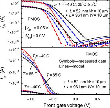
This method is mainly suitable for the measurement of carrier mobility in the inversion layer of MOSFET operating at room temperature. When a general MOSFET works at high temperature, the drain-source current Ids is equal to the sum of the channel current Ich and the leakage current Ir, but when it works at room temperature, the leakage current Ir decreases sharply and is approximately zero, making the drain-source current Ids is the channel current Ich. Therefore, the carrier mobility of the general MOSFET inversion layer can be obtained by measuring the I-V characteristics of the linear region.
Summary
To sum up, a total of 7 measurement methods of carrier mobility are pointed out. In addition, drift experiments, analysis of ion diffusion, and analysis of pyroelectric current can also be used. Carrier mobility is measured by methods such as polarized charge transient response.
Latest: Output power
Next: DVD-5


